- Electronic properties of transition metal dichalcogenides
 Transition metal dichalcogenides offer the fascinating possibility of producing relatively large area semiconductors of single molecular layer thickness which may be fabricated into nanoscale device structures utilizing their optical, electronic or spin properties. We are studying the band structure of layered semiconductors of the transition metal dichalcogenide family based on ReS2 and ReSe2, using angle-resolved photoemission at the SOLEIL synchrotron in Paris combined with density functional theory calculations carried out using high performance computing facilities in Bath. We are using this to gain a better understanding of charge transport in these materials.
- Supervisor(s)
- Dr. Daniel Wolverson, University of Bath
- Optical properties of transition metal dichalcogenides
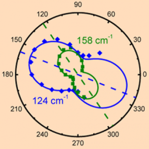 Linked to the above studies of the electronic band structure and charge transport in ReSe2 and ReS2, we have also made extensive studies of Raman scattering (the inelastic scattering of light by phonons) in these materials, together with DFT calculations of the phonon dispersion and Raman scattering cross-sections. This enables us to determine crystal orientation, essential for all applications, and we are now probing the effect of dopants on the lattice dynamics.
- Supervisor(s)
- Dr. Daniel Wolverson, University of Bath
- Nonlinear photonics with 2D materials: Manipulating light on a surface
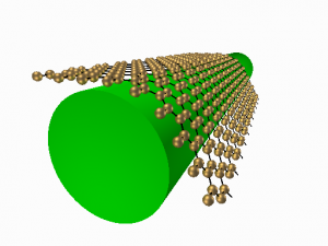 Newly emerging 2D materials exhibit interesting optical and opto-electronic properties. In particular, their extraordinary high nonlinear optical response creates fascinating opportunities for applications in light frequency conversion, all-optical signal processing and single photon sources. We are developing theoretical and numerical tools and analyse nonlinear and quantum optical processes in such novel photonic structures with integrated 2D materials.
- Supervisor(s)
- Dr. Andriy Gorbach, University of Bath
- Anisotropic electronic properties and transport in graphene and other 2D materials
 We exploit the unconventional physics of graphene – a gap-less material, governed, unlike conventional quantum systems, by the relativistic, Dirac equation –to induce anisotropic electron transport. By subjecting 2D graphene sheets to external, atomically-controlled potentials we aim to guide electrons in tailored directions, similar to how optical fibres guide light; or, on the contrary, confine them. Atomically-resolved scanning probe microscopies are used to both probe and induce such effects. We extend such approaches to low-symmetry transition metal dichalcogenides: unlike graphene, these have sizeable bandgaps, while their anisotropy is structural (and not of quantum origin).
- Supervisor(s)
- Dr. Adelina Ilie, University of Bath
- Atomic scale tailoring of transition metal dichalgogenides for spintronic and magnetic applications
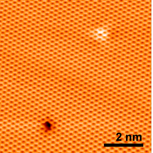 2D Transition metal dichalcogenide (TMD) semiconductors with large spin-orbit interaction and spin-valley coupling have strong potential for spintronics and valleytronics – fields exploiting carriers’ spin and valley (property arising from crystal symmetry) degrees of freedom. Utilising these intrinsic properties, we explore ways to induce spin-polarization within single and few-layers of such TMDs. Moreover, these materials also display the potential for magnetic properties through atomic scale engineering. Using primarily scanning probe microscopy and spectroscopy (correlated with theoretical simulations by collaborative groups), we also probe and tailor local magnetic moments, and aim for long-range magnetic order, to create new nanomagnetic semiconducting materials.
- Supervisor(s)
- Dr. Adelina Ilie, University of Bath
- Topological effects in bilayer graphene
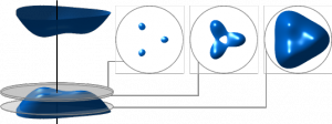 The shape of the Fermi surface is crucial for understanding the electronic properties of metals and changes in its topology causes anomalous behaviour of many physical properties. Bilayer graphene is a very special material in that, unlike a metal, the shape of its Fermi surface can be tuned by external means. We are trying to understand theoretically the interplay between topology of the single-particle spectrum and many-body interactions and its effect on electronic and transport properties.
- Supervisor(s)
- Dr. Marcin Mucha-Kuczynski, University of Bath
- Van der Waals heterostructures
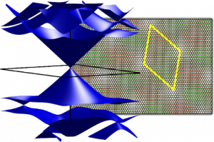 Two-dimensional crystals can be stacked on top of each other in a desired sequence to build new artificial materials layer by atomic layer. We study theoretically the novel electronic properties of van der Waals heterostructures arising from the interplay of properties of individual layers, such as graphene and hexagonal boron nitride.
- Supervisor(s)
- Dr. Marcin Mucha-Kruczynski, University of Bath
- Physical properties of 2D atomic crystals
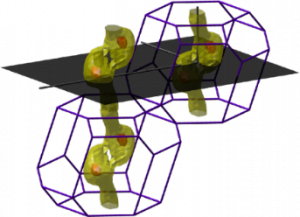 2D atomic crystals are a group of new, atomically thin materials that includes graphene. We study theoretically the physical properties to answer questions such as what happens to more exotic electronic phases (e.g. superconductivity, charge density waves) when a bulk piece of material is reduced to several atomic layers, how can the properties of 2D crystals be tuned (for example, by strain, electrostatic gating or chemical functionalization) and what is the link between the electronic properties and structural phases?
- Supervisor(s)
- Dr. Marcin Mucha-Kruczynski, University of Bath
- Nonlocal atomic manipulation
 We use the scanning tunnelling microscope to image and manipulate individual atoms and molecules. Instead of manipulating only the atom that is directly in the microscope’s sights (as others have done), leading to a one-atom-at-a-time limit, we have pioneered nonlocal manipulation where the effect of the injected electric current is spread across a surface over distances of 10’s of nanometers. This nonlocal process allows thousands of individual molecules to be manipulated simultaneously. We explore from the `classical’ hot-electron regime, to the coherent quantum limit.
- Supervisor(s)
- Dr. Peter Sloan, University of Bath
- Single Molecule Physics
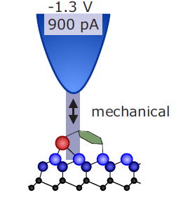 The scanning tunnelling microscope (STM) has given unprecedented measurement and control of single atoms and molecules at a surface. Perhaps its most unique ability lies in instigating single molecule reactions and imaging the outcome but experiments are limited by time and the probabilistic nature of quantum mechanics. We use a computer controlled experimental automation to go beyond the normal 10 or 20 experimental results, and gather data on 100s and 1000s of individual manipulation event. This allows us to rigorously measure over a wide range of parameters what the true influence of the STM in these single molecule reactions really is, often with surprising results
- Supervisor(s)
- Dr. Peter Sloan, University of Bath
- Characterisation and functionalization of graphene and 2D materials
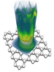 Graphene and other 2D materials, such as hexagonal boron nitride or 2D chalcogenides, have extraordinary electronic, optical and magnetic properties; they will be the basis of future nanotechnologies. Cutting-edge characterization is required to investigate the properties of such atomically thin structures. The University of Bristol has recently installed a state-of-the-art NanoESCA, a UHV instrument that is able to image and quantify the properties of these materials. The chemical composition is being investigated by means of XPS/XPEEM, the atomic structure by SPA-LEED and the electronic band structure by µ-ARPES.
We are currently working with Eindhoven University of Technology on hydrogenated graphene and also collaborating with the National Physical Laboratory (NPL) who are providing CVD-grown graphene and related 2D materials with controlled defect size and density. The work is focused on selected-area µ-ARPES to establish the correlation between defects and electronic structure. The µ-ARPES can also be employed to understand the orientation of the 2D materials across individual domains at grain boundaries.
- Supervisor(s)
- Dr. Neil Fox and Mr Mattia Cattelan, University of Bristol
