These are some PhD project themes which exemplify the range of subjects covered by the CDT. You will select your actual PhD research project during your first year. The projects on offer will be more extensive than those described in this example list.
Superconductivity
- Research on superconductivity in the CDT is wide ranging, spanning fundamental studies of the origin of the pairing interaction and other competing phases, across theory and the fabrication of novel devices.
-
- Imaging competing orders in high TC cuprates
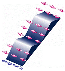 High temperature superconductivity (HTS) in layered cuprates occurs in the proximity of other ordered phases with broken symmetry. These include the “pseudogap” phase, spin-density wave order and (recently discovered) charge density wave order. Understanding the relationship of these competing (or possibly promoting) phases will be key to unravelling the origin the HTS phenomenon. We use x-ray and neutron scattering to investigate the nature of the competing phases. Experiments are performed at synchrotrons and neutron facilities in Europe and beyond.
- Supervisor(s)
- Professor Stephen Hayden, University of Bristol
- Superconducting energy gap structure
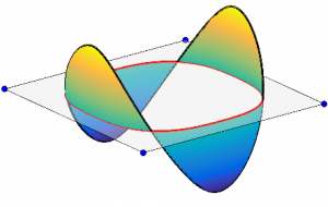 The structure of the superconducting energy gap D(k) is perhaps our most informative window on the structure of the interactions which cause electron pairing and hence superconductivity. To determine DD we use a combination of measurements of magnetic penetration depth and specific heat conducting at temperatures down to 0.04K, using custom built apparatus. Specific heat measurements are extended to very high fields (>30T) at the HMFL Nijmegen. State of the art single crystal samples are grown at Bristol and by collaborators in Kyoto, Stanford and Munich.
- Supervisor(s)
- Professor Antony Carrington, University of Bristol
- Electronic structure using quantum oscillations
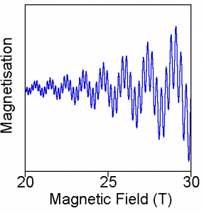 Magneto-quantum oscillations are a powerful probe of electronic structure, giving precise information about the quasiparticle properties and structure of the Fermi surface. Measurements are conducted at low temperature and very high magnetic fields both in Bristol and at international high magnetic field centres (Toulouse, Nijmegen, and Tallahassee). A particular theme is using pressure to tune the properties of the superconductor, allowing different regions of the phase diagram to be investigated systematically using a single sample and without introducing disorder.
- Supervisor(s)
- Professor Antony Carrington and Dr. Sven Friedemann, University of Bristol
- Magnetic imaging in unconventional superconductors
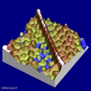 The properties of superconductors in a magnetic field, in particular the behaviour of vortex matter, can reveal important information about unconventional forms of electron pairing as well as the electronic band-structure near the Fermi surface. Magnetic imaging using nanoscale scanning Hall probes is performed at temperatures down to 300mK to identify the signatures of novel superconducting condensates. For example, order parameters that break time reversal symmetry can lead to spontaneous chiral currents (magnetic fields) and unusual vortex phenomena.
- Supervisor(s)
- Professor Simon Bending, University of Bath
- Superconducting spintronics
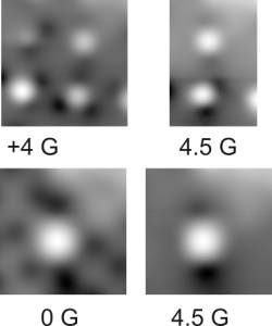 Novel superconducting pair correlations can be formed at superconductor-ferromagnet (S-F) interfaces where spin degeneracy is broken. The conversion of conventional spin singlet Cooper pairs into spin triplet pairs at an S-F interface with non-collinear magnetisation is being explored in novel spintronic devices. The non-collinear magnetisation structure found in spin valves, magnetic vortices and other more complex spin textures such as skyrmions, is being exploited to optimise and control triplet pair generation.
- Supervisor(s)
- Professor Simon Bending, University of Bath
- Gate-induced superconductivity in 2D materials
 New correlated electron states can be induced in molecular layers of so-called ‘2D materials’ by very high carrier doping. Field effect ‘doping’ with ionic liquid gates is being used to induce very high charge densities in few-layer graphene and transition metal dichalcogenide samples, allowing the evolution of insulating, metallic and superconducting states to be systematically tracked. Other types of correlated electron phases such as ferromagnetism and charge density waves are being sought at extremely high carrier densities.
- Supervisor(s)
- Professor Simon Bending, University of Bath
- Modulation of low carrier density superconductivity with light
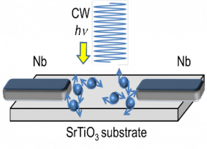 SrTiO3 is an extremely unusual superconductor because of its very low carrier density. The ratio of the Fermi temperature to the superconducting energy gap approaches unity. This low density means that very substantial changes to the properties can be engineered by illuminating the same with visible light. This allows the production of light-tunable superconducting devices which are fabricated with e-beam lithography.
- Supervisor(s)
- Dr. Chris Bell, University of Bristol
- Spin and heat currents in superconductors
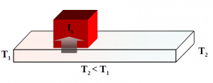 Traditionally superconductors were considered incompatible with magnetism. This view has been revised in recent year as more and more aspects of superconductivity have emerged where it is intertwined with magnetism. One particular aspect we are working on is the theory of generation of spin polarised currents in superconductors via the application of temperature gradients. This combination of the potential use of heat losses to effectively create spin polarised currents used in magnetic storage devices is fundamental basic research aiming for long term applications.
- Supervisor(s)
- Dr. Martin Gradhand, University of Bristol
-
- Graphene with proximity-induced superconductivity
 The superconducting order in a superconductor does not decay infinitely quickly at the surface. As a result, its paired state can be carried over to an adjacent normal metal – a phenomenon known as the proximity effect. We are currently studying theoretically the electronic and optical properties of graphene with proximity-induced superconductivity in order to establish whether optical probes can distinguish between the possible order parameters that can be induced in graphene.
- Supervisor(s)
- Dr. Marcin Mucha-Kruczynski, University of Bath
Strongly Correlated Electron Systems
- Here we group research themes based on materials where strong correlation does not result in superconductivity, but instead other interesting ground states such as Mott or Kondo insulators and heavy Fermion behaviour.
-
- Quantum order in oxide materials
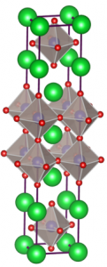 Layered 3d, 4d and 5d oxides such as cuprate, ruthenates, and iridates offer an interesting playground to tune effects of electronic bandwidth, electronic correlations, exchange interactions and spin-orbit coupling. We study new electronically ordered phases at low temperature. A recent example [Nature Materials 14, 373-378 (2015)] is Sr3Ru2O7 where an 8T magnetic field induces a spin-density wave and results in a novel ‘nematic’ phase with very anisotropic electronic properties. The phase arises from competing magnetic interactions. We investigate this and other phases by applying uniaxial stress and magnetic field. Measurements are conducted with a combination of x-ray, neutron scattering, transport and thermodynamic measurements.
- Supervisor(s)
- Professor Stephen Hayden, University of Bristol
- High-pressure studies of correlated materials
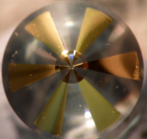 High pressure can be exploited as a unique parameter with which to tune the electronic properties of strongly correlated electron materials. By changing the lattice parameters with pressure, we adjust the overlap between atomic orbitals and hence change the electronic structure – for example changing an insulating material into a good conductor. The challenge is to combine such high pressures (achieved with diamond anvils for example) with precision measurements at very high magnetic fields and low temperatures.
Recently we managed, for the first time, to directly measure the Fermi surface of a Mott insulator in its high-pressure metallic state. To do this we used an anvil cell, like the one pictured, combined with a contactless radio frequency technique to measure quantum oscillations in fields close to 40T. We interpret our data using density function theory band-structure calculations.
- Supervisor(s)
- Dr. Sven Friedemann, University of Bristol
Novel Magnetic Materials and Devices
- Modelling realistic spintronic devices
 Over the last 15 years many new effects connecting charge and spin transport of electrons have been identified which harness relativistic spin-orbit coupling to create spin currents in non-magnetic materials. Recently, these effects have been realised in real devices such as magnetic random access memories (MRAM). In our work, we theoretically model these effects in real devices, taking into account disorder, interfaces, and finite temperatures from first principles. In order to achieve this, we develop bespoke in house computer codes describing the relativistic electronic structure and apply this to devices actually measured by our collaborators.
- Supervisor(s)
- Dr. Martin Gradhand, University of Bristol
- Single molecule electronics
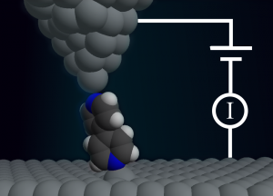 Single molecule electronics represents the ultimate in miniaturization, where circuit elements are replaced by individual molecules. It is already possible to contact individual molecules electrically using a scanning probe microscope to measure their conductance. It is even possible to make them act like a transistor by gating them electrochemically. Single or few-molecule devices are unlikely to replace circuits based on inorganic semiconductors any time soon, but they already have properties that make them of interest for sensors. Furthermore the physics involved in charge and spin transport through molecules and across their contacts is fascinating, and much remains unknown. Within the CDT-CMP, we offer projects probing new aspects of single molecule electronics exploiting our unique experience of working with magnetic metal and semiconductor contacts. This enables us to go beyond single molecule electronics to probe spintronic and photoelectronic effects
- Supervisor(s)
- Professor Walther Schwarzacher, University of Bristol
- Collective spin excitations measured with resonant inelastic X-ray scattering
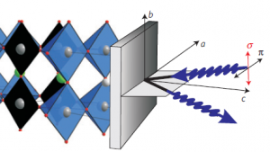 Resonant inelastic x-ray scattering (RIXS) is a new technique to measure collective magnetic excitations in solids such antiferromagnets, quantum magnets and superconductors. RIXS offers the possibility to study collective electronic excitations up to high energies (~eV) with a resolution of tens on meV on samples of size 10 micrometres. State-of-the-art new RIXS spectrometers are available at the Diamond light source in the UK and the ESRF in France. We apply RIXS and neutron scattering techniques to study the collective magnetic excitations in topical systems such as iron-based and cuprate superconductors, frustrated magnets, and magnetic transition-metal oxide systems.
- Supervisor(s)
- Professor Stephen Hayden, University of Bristol
- New transition metal monochalcogenides
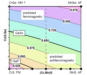 There have been many attempts to introduce magnetism into semiconductors, but the search is still on for room temperature ferromagnetic materials compatible with semiconductor electronics. The figure shows density functional theory (DFT) predictions of magnetic phases of thin layers of new transition metal chalcogenides (not found in nature) being grown by molecular beam epitaxy by collaborators at Heriot-Watt University. Optical spectroscopy, Raman scattering, magneto-optics and charge transport studies (with Prof. Simon Bending, Bath) are being used to investigate these materials, along with DFT simulations.
- Supervisor(s)
- Dr. Daniel Wolverson, University of Bath
Power Electronics and Devices
- Thermal management of semiconductor devices
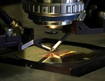 Advanced high power electronic devices require detailed knowledge of how power is generated and dissipated in the devices at a microscopic scale. We study this using both experiment, notably micro-Raman spectroscopy, and simulation in a variety of different structures including those based on Gallium Nitride, Silicon Carbide and Diamond.
We work closely with companies who develop power electronic devices such as with NXP, ONSemi, TriQuint and others.
- Supervisor(s)
- Professor Martin Kuball, University of Bristol
- Isotopic diamond for radiation conversion devices
 The growth of isotopically pure multi-layers of Carbon 12 and Carbon 13 diamond by Chemical Vapour Deposition (CVD), is a key capability to construct new types of semiconducting diamond devices for electron multiplication and radiation conversion. Carbon13 diamond is an interesting material because it is harder than Carbon12 and has an electronic band gap 17meV larger than Carbon12. This energy difference between Carbon12 and Carbon13 layers allows charge carriers to be confined within the Carbon 12 material, which can be a useful property in many electronic devices. We use a prototype DC Plasma reactor to grow isotopically pure diamond material at high growth rates. The growth system operates at higher pressures and higher electrical powers than the other five diamond reactors we operate which alters the density and distribution of impurity and point defects present in CVD diamond. Diamond on diamond structures are being explored that employ Carbon 12, 13 layers to evaluate the carrier transport, electron multiplication and radiation absorption properties for device applications. This system is also being used to conduct experiments to determine an approach for making Carbon 14 diamond by CVD
- Supervisor(s)
- Dr. Neil Fox and Professor Paul May , University of Bristol
Optoelectronics and Novel Materials
- Electron transport properties of novel organic crystals
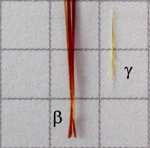 Single crystals are interesting for electronic applications because careful synthesis can ensure high purity and long-range order, but conductivities tend to be low. In order to improve carrier mobilities in organic crystals, the molecular configuration needs to be altered without the addition or subtraction of chemical substituents, which may adversely affect the conductive properties. We are achieving this by synthesising organic crystals previously unknown to science through the application of strong magnetic fields during their growth. In collaboration with the High Field Magnet Laboratory in Nijmegen, and the Laser Chemistry, Spectroscopy & Dynamics Group in Bristol, we create and test these crystals under applied fields of up to 37 T.
- Supervisor(s)
- Dr. Simon Hall, University of Bristol
- Terahertz photonics
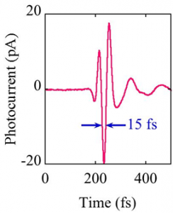 The terahertz (THz) part of the electromagnetic spectrum, which lies between microwaves and the infrared overlaps fundamental excitations in condensed matter. Studying the THz dynamics of materials yields unique information about the physics governing their macroscopic behaviour but optical devices at THz frequencies that can be used for spectroscopy are underdeveloped. We are using nano- and micro-structuring of semiconductors and glasses to create high performance components such as ultrafast and ultrabroadband sources, detectors, waveguides and polarisers.
- Supervisor(s)
- Dr. Steve Andrews, University of Bath
- Ultrafast spectroscopy of phase change materials
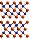 Femtosecond pulses of light can be used to excite and probe transient electronic and structural changes in materials that exhibit phase transitions (e.g. insulator to metal). Currently we are collaborating with the Singapore University of Technology and Design to use short and intense pulses of far-infrared radiation to drive and study phase transitions in GeTe/Sb2Te3 van der Waals superlattices that exhibit unusual properties such as giant magnetoresistance associated with topological insulator behaviour and applications to non-volatile memory and optical recording
- Supervisor(s)
- Dr. Steve Andrews, University of Bath
- Computational electronic structure
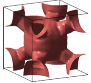 Density-functional theory has revolutionised the computation of the electronic structure of solids. Here in Bristol we use our high-performance computing facility, BlueCrystal, to calculate the electronic structure of electronically complex materials using a variety of state-of-the-art approaches (including FP-LAPW and KKR). Current themes include the study of the electronic structure of high-entropy alloys (a new alloy paradigm with typically 4 or 5 components in equiatomic concentrations), Heusler alloys (including half-metallic ferromagnets), and correlated oxides (such as manganites and ruthenates).
- Supervisor(s)
- Professor Stephen Dugdale, University of Bristol
- Electronic structure through momentum distributions
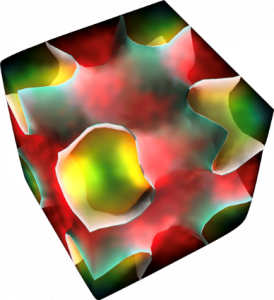 The electron momentum distribution contains a wealth of information about the ground state wave functions of electrons in solids. We can probe it through the Compton scattering of x-rays, and also by annihilating electrons with positrons. In particular, the momentum distribution holds valuable information about the Fermi surface, the shape of which is key to understanding many behaviours (e.g. magnetic ordering, density waves, electron-phonon coupling). We do positron annihilation in Bristol and with collaborators in Munich, and perform our Compton scattering experiments at the SPring-8 synchrotron in Japan.
- Supervisor(s)
- Professor Stephen Dugdale, University of Bristol
Single Atomic Layer Crystals (Graphene and Related 2D Materials)
- Electronic properties of transition metal dichalcogenides
 Transition metal dichalcogenides offer the fascinating possibility of producing relatively large area semiconductors of single molecular layer thickness which may be fabricated into nanoscale device structures utilizing their optical, electronic or spin properties. We are studying the band structure of layered semiconductors of the transition metal dichalcogenide family based on ReS2 and ReSe2, using angle-resolved photoemission at the SOLEIL synchrotron in Paris combined with density functional theory calculations carried out using high performance computing facilities in Bath. We are using this to gain a better understanding of charge transport in these materials.
- Supervisor(s)
- Dr. Daniel Wolverson, University of Bath
- Optical properties of transition metal dichalcogenides
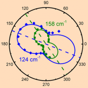 Linked to the above studies of the electronic band structure and charge transport in ReSe2 and ReS2, we have also made extensive studies of Raman scattering (the inelastic scattering of light by phonons) in these materials, together with DFT calculations of the phonon dispersion and Raman scattering cross-sections. This enables us to determine crystal orientation, essential for all applications, and we are now probing the effect of dopants on the lattice dynamics.
- Supervisor(s)
- Dr. Daniel Wolverson, University of Bath
- Nonlinear photonics with 2D materials: Manipulating light on a surface
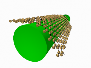 Newly emerging 2D materials exhibit interesting optical and opto-electronic properties. In particular, their extraordinary high nonlinear optical response creates fascinating opportunities for applications in light frequency conversion, all-optical signal processing and single photon sources. We are developing theoretical and numerical tools and analyse nonlinear and quantum optical processes in such novel photonic structures with integrated 2D materials.
- Supervisor(s)
- Dr. Andriy Gorbach, University of Bath
- Anisotropic electronic properties and transport in graphene and other 2D materials
 We exploit the unconventional physics of graphene – a gap-less material, governed, unlike conventional quantum systems, by the relativistic, Dirac equation –to induce anisotropic electron transport. By subjecting 2D graphene sheets to external, atomically-controlled potentials we aim to guide electrons in tailored directions, similar to how optical fibres guide light; or, on the contrary, confine them. Atomically-resolved scanning probe microscopies are used to both probe and induce such effects. We extend such approaches to low-symmetry transition metal dichalcogenides: unlike graphene, these have sizeable bandgaps, while their anisotropy is structural (and not of quantum origin).
- Supervisor(s)
- Dr. Adelina Ilie, University of Bath
- Atomic scale tailoring of transition metal dichalgogenides for spintronic and magnetic applications
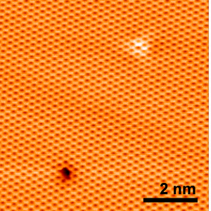 2D Transition metal dichalcogenide (TMD) semiconductors with large spin-orbit interaction and spin-valley coupling have strong potential for spintronics and valleytronics – fields exploiting carriers’ spin and valley (property arising from crystal symmetry) degrees of freedom. Utilising these intrinsic properties, we explore ways to induce spin-polarization within single and few-layers of such TMDs. Moreover, these materials also display the potential for magnetic properties through atomic scale engineering. Using primarily scanning probe microscopy and spectroscopy (correlated with theoretical simulations by collaborative groups), we also probe and tailor local magnetic moments, and aim for long-range magnetic order, to create new nanomagnetic semiconducting materials.
- Supervisor(s)
- Dr. Adelina Ilie, University of Bath
- Topological effects in bilayer graphene
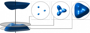 The shape of the Fermi surface is crucial for understanding the electronic properties of metals and changes in its topology causes anomalous behaviour of many physical properties. Bilayer graphene is a very special material in that, unlike a metal, the shape of its Fermi surface can be tuned by external means. We are trying to understand theoretically the interplay between topology of the single-particle spectrum and many-body interactions and its effect on electronic and transport properties.
- Supervisor(s)
- Dr. Marcin Mucha-Kuczynski, University of Bath
- Van der Waals heterostructures
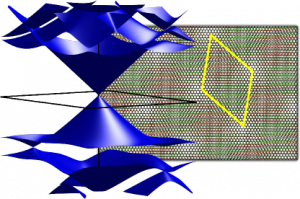 Two-dimensional crystals can be stacked on top of each other in a desired sequence to build new artificial materials layer by atomic layer. We study theoretically the novel electronic properties of van der Waals heterostructures arising from the interplay of properties of individual layers, such as graphene and hexagonal boron nitride.
- Supervisor(s)
- Dr. Marcin Mucha-Kruczynski, University of Bath
- Physical properties of 2D atomic crystals
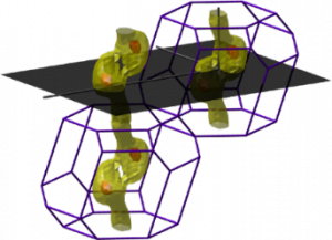 2D atomic crystals are a group of new, atomically thin materials that includes graphene. We study theoretically the physical properties to answer questions such as what happens to more exotic electronic phases (e.g. superconductivity, charge density waves) when a bulk piece of material is reduced to several atomic layers, how can the properties of 2D crystals be tuned (for example, by strain, electrostatic gating or chemical functionalization) and what is the link between the electronic properties and structural phases?
- Supervisor(s)
- Dr. Marcin Mucha-Kruczynski, University of Bath
- Nonlocal atomic manipulation
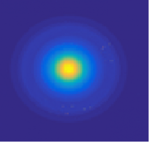 We use the scanning tunnelling microscope to image and manipulate individual atoms and molecules. Instead of manipulating only the atom that is directly in the microscope’s sights (as others have done), leading to a one-atom-at-a-time limit, we have pioneered nonlocal manipulation where the effect of the injected electric current is spread across a surface over distances of 10’s of nanometers. This nonlocal process allows thousands of individual molecules to be manipulated simultaneously. We explore from the `classical’ hot-electron regime, to the coherent quantum limit.
- Supervisor(s)
- Dr. Peter Sloan, University of Bath
- Single Molecule Physics
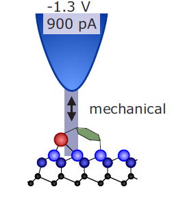 The scanning tunnelling microscope (STM) has given unprecedented measurement and control of single atoms and molecules at a surface. Perhaps its most unique ability lies in instigating single molecule reactions and imaging the outcome but experiments are limited by time and the probabilistic nature of quantum mechanics. We use a computer controlled experimental automation to go beyond the normal 10 or 20 experimental results, and gather data on 100s and 1000s of individual manipulation event. This allows us to rigorously measure over a wide range of parameters what the true influence of the STM in these single molecule reactions really is, often with surprising results
- Supervisor(s)
- Dr. Peter Sloan, University of Bath
- Characterisation and functionalization of graphene and 2D materials
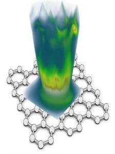 Graphene and other 2D materials, such as hexagonal boron nitride or 2D chalcogenides, have extraordinary electronic, optical and magnetic properties; they will be the basis of future nanotechnologies. Cutting-edge characterization is required to investigate the properties of such atomically thin structures. The University of Bristol has recently installed a state-of-the-art NanoESCA, a UHV instrument that is able to image and quantify the properties of these materials. The chemical composition is being investigated by means of XPS/XPEEM, the atomic structure by SPA-LEED and the electronic band structure by µ-ARPES.
We are currently working with Eindhoven University of Technology on hydrogenated graphene and also collaborating with the National Physical Laboratory (NPL) who are providing CVD-grown graphene and related 2D materials with controlled defect size and density. The work is focused on selected-area µ-ARPES to establish the correlation between defects and electronic structure. The µ-ARPES can also be employed to understand the orientation of the 2D materials across individual domains at grain boundaries.
- Supervisor(s)
- Dr. Neil Fox and Mr Mattia Cattelan, University of Bristol
