Thermal management of semiconductor devices
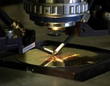
 Advanced high power electronic devices require detailed knowledge of how power is generated and dissipated in the devices at a microscopic scale. We study this using both experiment, notably micro-Raman spectroscopy, and simulation in a variety of different structures including those based on Gallium Nitride, Silicon Carbide and Diamond.
We work closely with companies who develop power electronic devices such as with NXP, ONSemi, TriQuint and others.
Supervisor(s)Professor Martin Kuball, University of Bristol
- Isotopic diamond for radiation conversion devices
 The growth of isotopically pure multi-layers of Carbon 12 and Carbon 13 diamond by Chemical Vapour Deposition (CVD), is a key capability to construct new types of semiconducting diamond devices for electron multiplication and radiation conversion. Carbon13 diamond is an interesting material because it is harder than Carbon12 and has an electronic band gap 17meV larger than Carbon12. This energy difference between Carbon12 and Carbon13 layers allows charge carriers to be confined within the Carbon 12 material, which can be a useful property in many electronic devices. We use a prototype DC Plasma reactor to grow isotopically pure diamond material at high growth rates. The growth system operates at higher pressures and higher electrical powers than the other five diamond reactors we operate which alters the density and distribution of impurity and point defects present in CVD diamond. Diamond on diamond structures are being explored that employ Carbon 12, 13 layers to evaluate the carrier transport, electron multiplication and radiation absorption properties for device applications. This system is also being used to conduct experiments to determine an approach for making Carbon 14 diamond by CVD
- Supervisor(s)
- Dr. Neil Fox and Professor Paul May , University of Bristol
